Description
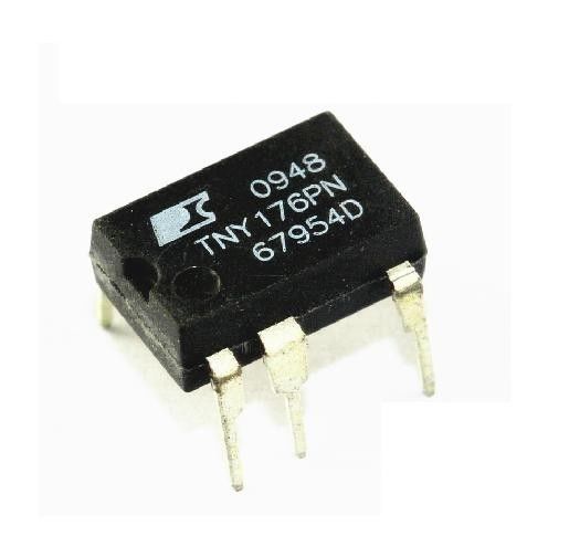
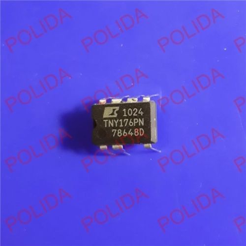
TNY176 incorporates a 650 V power MOSFET, oscillator, high voltage switched current source, current limit (user selectable) and thermal shutdown circuitry. The IC family uses an ON/OFF control scheme and offers a design flexible solution with a low system cost and extended power capability.
features

Drain Voltage ……………………………. …………..-0.3 V to 650 V
DRAIN Peak Current…………………720 (1350) mA
EN Voltage …………………………………………………. -0.3 V to 9 V
EN Current ………………………………………………………… 100 mA
BP/M Voltage ………………………………………….. ….-0.3 V to 9 V
Storage Temperature ………………………………..-65 °C to 150 °C
Operating Junction Temperature(3)……………..-40 °C to 150 °C
Operation
TNY176 devices operate in the current limit mode. When enabled, the oscillator turns the power MOSFET on at the beginning of each cycle. The MOSFET is turned off when the current ramps up to the current limit or when the DCMAX limit is reached. Since the highest current limit level and frequency of a TNY176 design are constant, the power delivered to the load is proportional to the primary inductance of the transformer and peak primary current squared. Hence, designing the supply involves calculating the primary inductance of the transformer for the maximum output power required. If the TNY176 is appropriately chosen for the power level, the current in the calculated inductance will ramp up to current limit before the DCMAX limit is reached.
Applications
• Chargers/adapters for cell/cordless phones, PDAs, digital
cameras, MP3/portable audio, shavers, etc.
• DVD/PVR and other low power set top decoders
• Supplies for appliances, industrial systems, metering,

Reviews
There are no reviews yet.